
CORPORATE HISTORY
Jiaxing Weifu Semiconductor Co., Ltd. was established in February 2017. Headquartered in Pinghu City, Jiaxing, Zhejiang, it currently has two R&D centers in Jiaxing/Shanghai.
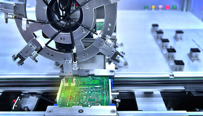
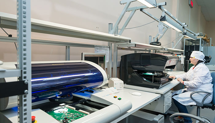
Weifu currently has mass production capabilities for wafer test CP and finished product test FT. Simulation product test platform (such as Beijing Huafeng Acoo, Hongce, Sinetest, Changchuan, etc.). Test platform for digital products (such as Chroma, S100, EVA100, German rate, etc.). CP test probe station (such as TSK UF200, TEL P8/P8XL/P12, 90A, UF300A, OPUS, etc.), can test 6 inch, 8 inch, and 12 inch integrated circuits. FT test sorting machine (such as Pillide, Zhongyi, Changchuan, etc.), can test SOP/TSSOP/SSOP/TO92 and other packaged products. FT test turret machines (such as Shenzhen Keda, Yingshuo, Bulk, etc.), can test SOP/QFN and other packaged products.
With the rapid development of China's semiconductor industry, Weifu will give full play to the advantages of its own professional team and expand into the integrated circuit service industry chain starting from wafer testing.


2012-2017
—
● Shanghai Weifu established and R&D center
● Serving and incubating small and medium-sized IC design companies
● Small-scale mass production service
● Saving core technology and industrial resources

2017-2018
—
● Jiaxing Weifu was established, "municipal-level entrepreneurial leading talent"
● Well-known investment institutions
● Jiaxing Phase I plant (wafer testing) was put into mass production
● Enter the mid-to-high-end memory and SOC integrated circuit market

2018-2020
—
Jiaxing R&D Center was established, a national high-tech enterprise
● Industry Guidance Fund
● The second phase of the Jiaxing plant project was launched, and it was used for the steady expansion of wafer testing, and
New business development such as finished product testing, reliability testing and high-end customized polishing
● Enter the IC market such as RF and Sensor

Copyright © All rights reserved by Jiaxing Weifu Semiconductor Co., Ltd.
Privacy Policy